Researchers built surfaces that direct the growth of nanowires and nanotubes and watched their growth process in real time. The forecast for the future: building advanced devices, such as tiny solar cells
Does our future lie in tiny materials? According to nanotechnology researchers, it may be. This field deals with systems whose size ranges from a few nanometers to tens of nanometers (nanometer = billionth of a meter, 100,000 times finer than a hair). Nanomaterials - with at least one nanometer dimension - are part of this field. Their physical properties - such as high electrical conductivity and acceleration of chemical reactions (catalysts) - depend on this size and are adapted to the production of a variety of advanced devices, for example electronic, digital, quantum and medical.
Prof. Ernesto Yuslevitz from the Department of Molecular Chemistry and Materials Science in the Faculty of Chemistry at the Weizmann Institute and his team deal with nanotechnology and nanomaterials - one-dimensional (nanotubes and nanowires made of carbon and semiconductors - materials that conduct electricity at room temperature - the building blocks of modern electronics), and two- dimensional (layered materials such as metals and graphene). Their goal is to discover new materials - their formation, properties, behavior and self-organization - so that in the future they can build a variety of devices from them.
Says Prof. Yoslevitz: "In the last decades, they discovered that when the material is nano-sized, its properties change accordingly and it is possible to transmit more information through it. In various systems, also in the human body, tiny tubes and wires have essential transfer functions, for example of materials, energy, power and information. Nanoscience has opened up to us a new world of materials and properties that we did not know until now, on the basis of which it is possible to develop devices of many different types. The thinner the wires and pipes, the more efficient systems can be built from them."
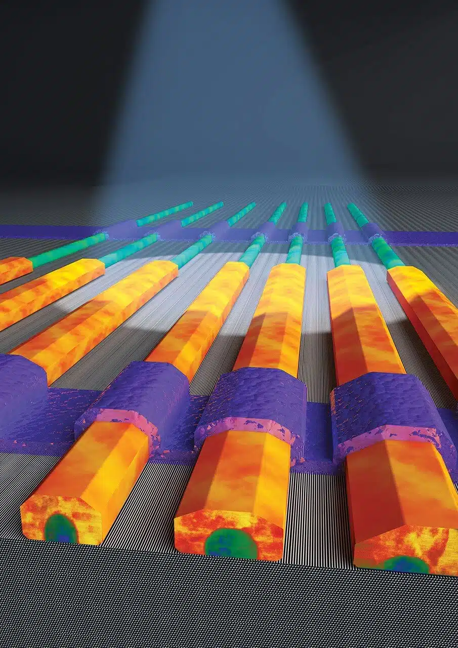
In their latest study, which won a research grant from the National Science Foundation, Prof. Youslevitz and his team wanted to test how nanowires and nanotubes grow in an orderly manner, so that their tangles are avoided and they can function as semiconductors. It is actually a "guided growth" - a process that makes it possible to grow ordered arrays of nanowires and nanotubes, control their size, diameter, direction and location, and thus build efficient devices based on them.
In the past, researchers discovered that when they grow nanowires and nanotubes on certain surfaces (for example, smooth and wrinkled crystals with artificial nanogrooves created by lithography or glass scratched using diamonds), they grow horizontally - according to the arrangement of the rows of atoms, nanogrooves or scratches, which are used as "rails". They also inject metal into these surfaces and put them into a heating element (temperature of 800 degrees). The nanowires and nanotubes grow out of the nanoparticles of the molten metal; It turns into a drop (liquid) that slides along the rails and thus leaves a trail behind it - which turns into semiconductor nanowires and tubes.
In their latest study, the researchers observed for the first time the guided growth process of the nanowires and nanotubes along the tracks with an electron microscope (with the help of the electron microscopy unit at the Weizmann Institute); An electron beam scanned them and the electrons emitted from them created images in which their growth could be observed. For example, it was discovered that when the drop of metal runs out, the wires and tubes stop growing and shrink back. "For the first time, we saw in real time how the nanowires and nanotubes grow on the surfaces, for example their trajectory and speed, explains Prof. Yoslevitz.

Watching the guided growth process in real time and understanding it will allow researchers to build advanced devices based on nanowires and nanotubes, such as transistors (electrical components used as electronic switches), physical components such as logic gates, light detectors and solar cells. "These devices could be used, for example, for the 'Internet of Things' (items embedded in sensors and software that enable advanced communication and information collection and analysis capabilities. For example, in medicine and smart transportation and a smart home)," concludes Prof. Yoslevitz.
Life itself:
Prof. Ernesto Yoslevitz, 54, married with four children (20, 17, 14, 14), lives in Rehovot. Born in Argentina and when he was nine years old he moved with his family to Barcelona, Spain. At the age of 18, he immigrated to Israel alone and enrolled in chemistry studies at the Hebrew University, where he also earned a doctorate. He did his post-doctorate at Harvard University and then joined the Weizmann Institute.

About two years ago, the archives of the Weizmann Institute found a telegram from 1919 that Chaim Weizmann sent to Jacob Yuslevitz - the founder of the Zionist Federation in Argentina in 1913 and owner of a metal factory - in which he asked him to raise funds for the Jewish Home in the Land of Israel. Prof. Yoslevitz, as it turned out, is the great-grandson of Jacob Yoslevitz. He says that "I discovered to my astonishment the connection between my great-grandfather and Weizmann, and it made me think that my work at the Weizmann Institute is a kind of closing a circle." He further adds that "in fact, my great-grandfather was already involved in materials 100 years ago in Argentina, my grandfather was a civil engineer, my father was an architect and designer and I am a nanomaterials person. That is, for four generations we have been producing buildings of different sizes."
More of the topic in Hayadan:
