This discovery is an important step in understanding the mechanisms that allow perovskite nanoparticles to heal themselves and paves the way for the integration of these materials in solar cells and other electronic devices.
When we are scratched or injured superficially, our body knows how to heal the wound by itself, or at most with the minimal help of a plaster or an antiseptic. Many research groups around the world are working on the development of materials with similar properties, which will know how to repair themselves without external help. We all know how frustrating it is to find out that the phone screen is broken and we have to replace it, and of course there are bigger problems - for example, a malfunction in the solar panels that drive a satellite in space. Now imagine that your screen and solar panel in space will know how to repair themselves and return to full function. Many research groups around the world are engaged in this challenge: the development of self-healing materials.
Positive news in this regard now comes from the research group of Dr. Yehondav Bekenstein from the Faculty of Materials Science and Engineering and the Solid State Institute at the Technion. Dr. Bekenstein and doctoral students Sasha Halpin and Noam Bar have developed semiconducting nanometer crystals, environmentally friendly, that know how to heal themselves. In an article in the journal Advanced Functional Materials They show how materials called "double perovskites" repair defects created in them following exposure to penetrating electron radiation.
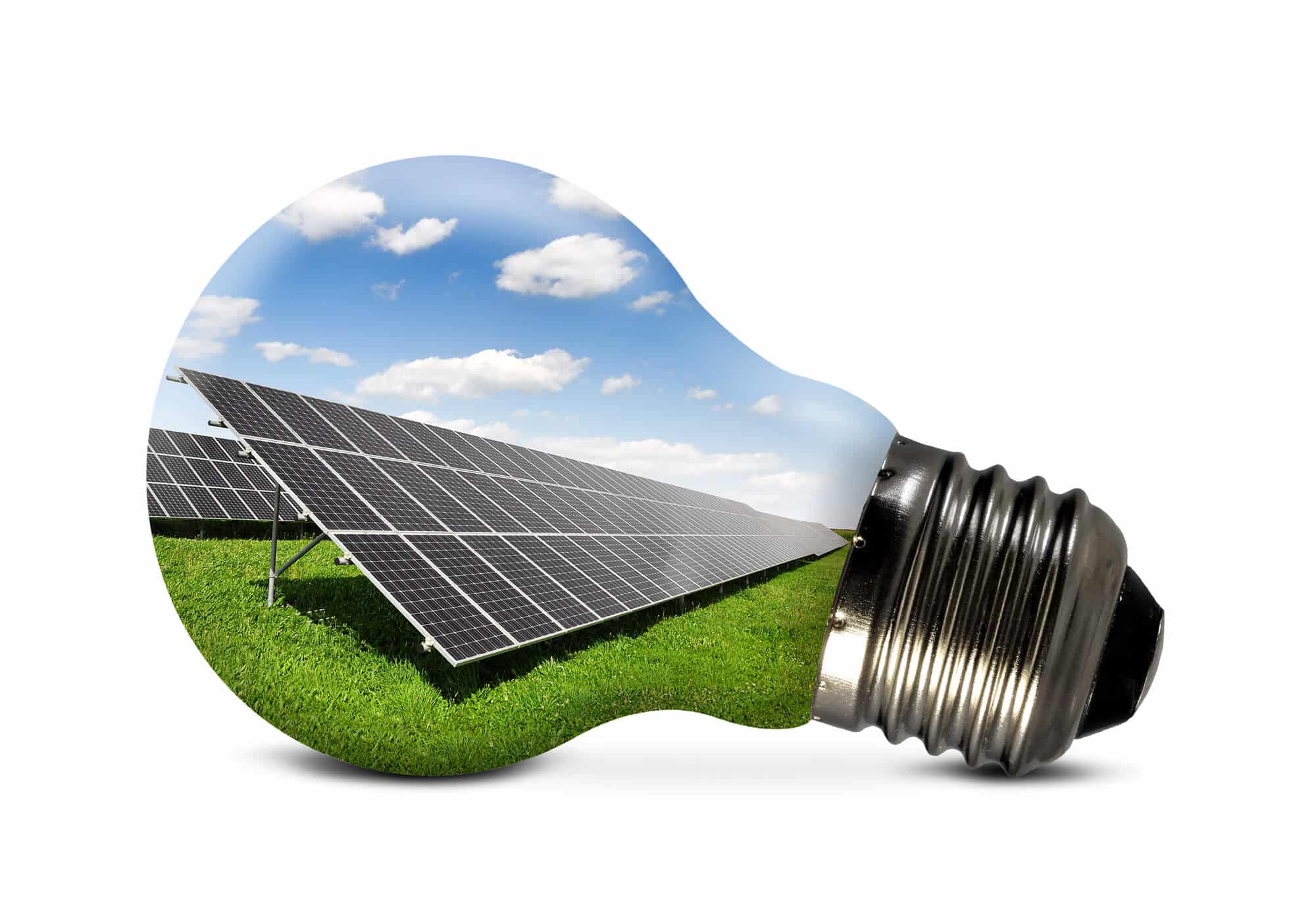
Perovskite materials have been known to science for more than a century, but only in recent years has it become clear that the group of lead-based halide perovskites are characterized by unique electro-optical properties that give them a huge advantage over silicon, for example high efficiency in converting solar energy into electricity. The perovskite is cheap to produce because it is produced and processed at relatively low temperatures compared to silicon, and it is possible to create flexible sheets from it that pave the way for a wide variety of applications. Double perovskites have an environmental advantage, as they may eliminate the use of lead, which is a highly toxic metal, currently incorporated into perovskite devices for energy conversion.
Dr. Beckenstein's research group specializes in the growth of nanometer perovskite crystals and the creation of perovskite surfaces with special physical properties. In the study described in Advanced Functional Materials The Technion researchers produced nanometer crystals in a short and simple process in the open air, while heating the material to 100 degrees Celsius. The researchers followed the crystals with a penetrating electron microscope and discovered that the powerful electron beam of the microscope created defects in them in the form of tiny internal spaces.
The researchers saw that the aforementioned spaces move around the center of the particle but avoid leaving the center towards its edges, as if a hidden wall blocks their way out. Based on the filming of dozens of videos and their computer analysis, the researchers were able to produce a picture of the dynamics taking place in the crystal in real time. They discovered that the said cavities are formed on the surface of the crystal, when the electron beam knocks atoms out of the material, but after their formation they migrate to equilibrium points inside the crystal. This migration, the researchers explain, is due to energetic reasons related to the presence of organic molecules covering the surface of the crystal. When they removed those molecules, the voids migrated to the surface of the crystal, and the inner region of the crystal recrystallized spontaneously back to its initial, defect-free state. In other words: The crystal healed itself.
This discovery is an important step in understanding the mechanisms that allow perovskite nanoparticles to heal themselves and paves the way for the integration of these materials in solar cells and other electronic devices.
The research was supported by the National Science Foundation, the Israel Innovation Authority, and TT (Alon Fellowship), the Russell Berry Institute for Nanotechnology at the Technion, and the Helen Diller Quantum Center at the Technion.
For the article in the Eת Advanced Functional Materials
More of the topic in Hayadan:

3 תגובות
It seems that soon we will see batteries that do not run out or with endless charging while self-healing damaged parts of the battery.
He is our son.
A side question that stems from pure curiosity: does anyone know if there is a connection between Yehondav Bekenstein and Yaakov Bekenstein, who is famous for the entropy of black holes?