Technion researchers have developed a smart light source based on a single atomic layer of material. The achievement will enable the development of new quantum applications in the field of computing and in other fields
Technion researchers have developed a new light source based on a single atomic layer. The innovative development, published in the journal Nature Nanotechnology, allows control ofSpin of the photons emitted in a two-dimensional material and paves the way for new photonic devices based on "spin optics on an atomic scale". The discovery is based on the interaction of a single atomic layer with nanoantenna arrays on a silicon chip while creating defects in photonic crystals.
The study was conducted in the research group of Prof. Erez Hasman, Head of the Laboratory for Atomic Scale Photonics, with Prof. Elad Koren, Head of the Laboratory for Electronic Nanomaterials and Nanocomponents at the Faculty of Materials Science and Engineering. The two research groups belong to the Helen Diller Quantum Center and the Russell Berry Nanotechnology Institute. The research was carried out and led by Dr. Kexiu Rong and Dr. Bo Wang in collaboration with researchers Dr. Elhanan Magid, Dr. Vladimir Kleiner, Avi Reuven, Bar Cohen and Shaul Katznelson.
What are two-dimensional materials? According to Prof. Korn, "In 2004, the possibility of creating a single atomic layer was first examined when the physicists Andre Geim and Konstantin Novoslov, later winners of the Nobel Prize in Physics (2010), developed a simple method for creating single layers of carbon atoms. The two attached adhesive paper to a piece of graphite and peeled off the material layer by layer until obtaining a single layer of atoms known as graphene. They showed that the atomic layer of matter is very different in its properties from the properties of matter in its three-dimensional form. It is a material a hundred times stronger than steel and with extraordinary electrical properties, and according to estimates it is expected to revolutionize conductors and semiconductors, displays and screens, solar cells and more. Following this discovery, atomic layers were developed from other materials, and they also exhibited surprising and unique properties."
Prof. Hasman continues and explains: "Following the discovery of graphene, many two-dimensional materials were discovered and studied, such as various semiconductors, which also make it possible to obtain interesting optical properties. Standard electronic chips are based on silicon, which greatly limits the development of the next generation of computers that requires a combination of electronics and photonics, partly due to the lack of an essential condition called 'direct energy gap' in silicon. To our surprise, the same direct energy gap was discovered in two-dimensional semiconductors, which makes it possible to combine photonics and electronics on the nanometer scale, to produce light sources and active photonic devices with them, and to pave the way for future generations of chips."
To minimize the electronic chip and significantly increase the speed of processing and the rate of information transmission, the accepted approach today is spintronics - performing operations on the spin, one of the important properties of the electron, and not on the electron flow. A few years ago Prof. Erez Hasman from the Technion founded a new field called Spinoptics, which makes it possible to utilize the spin of the photons through metasurfaces for the benefit of transferring and processing information in photonic chips. The transfer of information is based on controlling the photonic spin with the help of nanophotonics - optics on the nanometer scale.
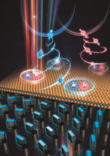
Two-dimensional semiconductor materials are characterized by energy levels whose emission depends on spin (spin valleys), this is due to the breaking of the mirror symmetry. The researchers at the Technion decided to take advantage of this feature and attach a single atomic layer of tungsten selenide (WSe2 For nanophotonics - nanoantennas that enable breaking symmetry in the photonic spin and obtaining a chip on an atomic scale that enables a light source and photonic devices while controlling and processing information in the photonic spin.
The researchers created a two-dimensional crystal structure from silicon that creates an energy gap in the emission field of the two-dimensional material so that the coupling of the atomic semiconductor to the photonic crystal blocks all optical emission channels from the two-dimensional material. By creating smart defects within the photonic crystal, controlling the phase of the defects using their geometry and coupling them, the researchers created a light source from a single atomic layer that separates and sorts the spins of the photons emitted from the two-dimensional semiconductor. This scientific discovery will make it possible to combine spintronics and spinoptics to develop a wide variety of devices on an atomic scale.
Prof. Hasman proudly notes that "this prestigious publication shows the importance of multidisciplinary research that combines physics, chemistry, materials science and engineering."
The research was supported by the National Science Foundation (ISF), the Ministry of Science and Technology, the Technion and the US Air Force Research Office. The components were realized at the Sara and Moshe Zisafel Center for Nanoelectronics (MNFU) at the Technion.
Lab sites: https://hasman.technion.ac.il/ https://koren.net.technion.ac.il/
for the article in Nature Nanotechnology click here
More of the topic in Hayadan:

2 תגובות
I don't really understand, but congratulations on the achievement!
When will we, finally, have the sentence "graphene is a material that is capable of doing a lot other than leaving the confines of the laboratory" shattered?