New research reveals a two-dimensional crystal system that allows unique control of its electrical charge through sliding between atomic layers. The new system creates atomically thick ladder steps of separate and well-defined electrical potentials, and may have a multitude of applications in industry in general and in information technologies in particular

New research reveals a two-dimensional crystal system that allows unique control of its electrical charge through sliding between atomic layers. The new system creates atomic-thick ladder steps of separate and well-defined electrical potentials, and may have a multitude of applications in industry in general and in information technologies in particular.
The research was conducted under the leadership of the team of researchers: Dr. Swaroop Dov, research student Noam Rab, Prof. Moshe Goldstein and Dr. Moshe Ben Shalom, from the School of Physics at Tel Aviv University, Dr. Wai Khao, Prof. Oded Hod and Prof. Michael Orbach from The Chemistry Department at Tel Aviv University, and Prof. Lior Kronik from the Weizmann Institute of Science.
The results of the study were published in the prestigious journal Nature.
Dr. Moshe Ben Shalom, head of the Laboratory for Layered Quantum Materials at the School of Physics explains: "We are very curious to find out how atoms decide to arrange themselves in matter, how the electrons choose to mix with each other and how the atomic order and the electric charge can be manipulated from the outside. These questions are difficult to answer because of the large amount of atoms and electrons in even today's smallest devices. One of the tricks is to study crystals, since their atoms are arranged in a periodic structure, so that the information about the entire system is determined by the properties of the one periodic cell - which includes a single number of atoms and electrons. And it is still difficult for us to understand and predict their order, because the electrons are spread over all the atoms at the same time and the properties of the quantum system are determined by all the particles together and the mutual relations between them."
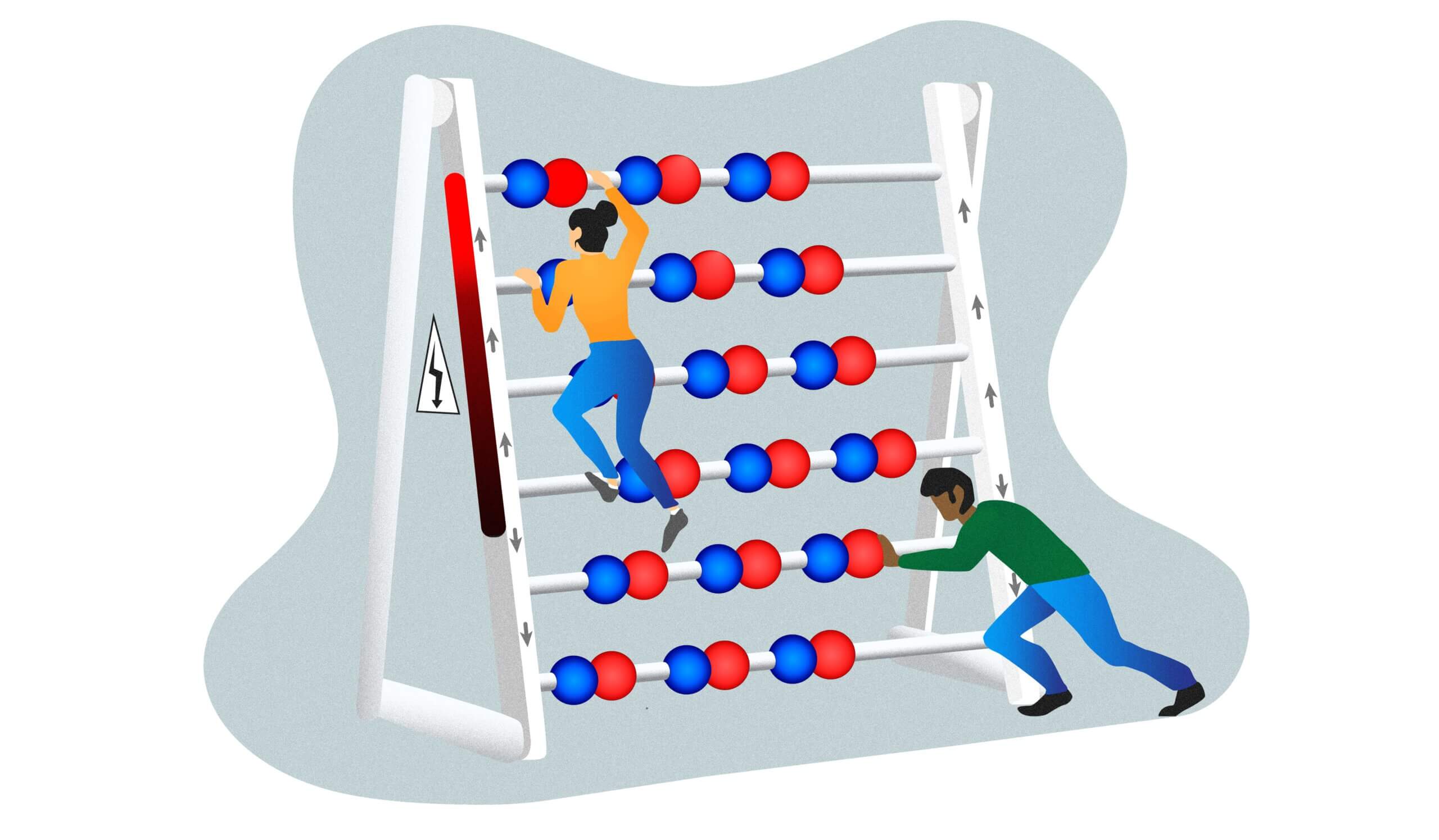
One way to discover the order of the atoms and the distribution of the electric charge is to break the symmetry of the structure, so that a constant internal electric field is created in the crystal. These crystals are called "polar" or polarized. In 2020, Dr. Ben Shalom's laboratory created a new polarized crystal by gluing two identical layers - where each layer is a single atom thick. Compared to the symmetrical crystals that grow in nature in which each new layer rotates to place atoms of one type exactly above the atoms of a second type, the researchers glued the pair of layers without the rotation - thus causing a tiny slip between the layers that breaks the symmetry, causes the electrons to jump from one layer to another, and creates electrical polarization internal. In a second step, the researchers discovered that it is possible to slide between the layers back and forth and thus switch the electrical polarization using an external electric field (see figure). They called the phenomenon SlideTronics.

"Slipping and climbing between electrical polarizations": The periodic crystal structure contains a pair of atoms at regular intervals in each horizontal layer. Each additional layer can be slid to the right or left in the horizontal plane to place a blue atom exactly above a red atom or vice versa, thereby bouncing electrons with an electric charge up or down between the layers. Unlike in polarized crystals known so far, the electric potential in the new system changes in a constant and well-defined value between each step. It is possible to climb in a controlled manner between all the different options, that is, it is possible to switch between the information units in the same crystal in contrast to a pair of modes in previous technologies.
Dr. Ben Shalom adds: "The new polarized crystal we discovered, only two atoms thick, is the thinnest possible and may be used in information technologies based on quantum tunneling. We are developing such tunneling units at Slide-Tro LTD, a company established by the university and an external investor and currently operating under the radar, and believe that the phenomenon enables a broad base for innovative electronic devices ranging from power reduction solutions to improved memory units. In terms of fundamental research, the discovery immediately raised new questions for us: How will the cargo be arranged? And what will be the size of the polarization? If we attach additional layers to the system in such a way that it breaks or preserves the symmetry?" "In other words, instead of thinning the thickness of the system by eating layers from the crystal, as was done until now, we could now stack polarized crystals layer by layer on top of each other and at the same time measure the magnitude of the polarization and the electric potential created at each step of the layer scale."
In the current experiment, the researchers were able to compare adjacent areas with a different number of layers stacked together with slips in different directions that create polarizations of different sizes. For example, for four layers (and three polarized contact surfaces) there are four options to arrange the direction of the three polarizations: all pointing up ↑↑↑, two up and one down ↑↑↓, one up and two down ↑↓↓ or three down ↓↓↓.
"Fortunately, we discovered a scale of well-defined polarizations separated by uniform polarization values, so that each step of the scale can be used as a separate unit of information," says Noam Rab, the research student who measured the crystals. "As mentioned, this is a reaction very different from that of the crystals known so far, where the surface reaction to polarization is significant and the change of polarization is possible as a single unit only - that is, changing the polarization in one layer changes the charge of all layers." Dr. Swarup Dov, lead author of the article, emphasizes: "We were also able to charge the layers with an additional electron for approximately every hundred atoms and thereby significantly improve the crystal conduction in the plane without damaging the perpendicular polarization." With the help of theoretical calculations based on the basic principles of quantum mechanics, we discovered that it is possible to design and build additional layered crystal combinations through relative sliding between the layers, and that the information about the polarization and symmetry of the system remains locked between the layers and protected from the environment," says Dr. Wai Chao is another lead author who did the calculations. "Actually, the 'Hakeltronica' helped us discover the thinnest polarization scale that can be built" concludes Dr. Ben Shalom. "A necessary continuation for future research is the manipulation of additional electronic orders, such as magnetic polarization and superconductivity through similar slippages between different crystal symmetries."
More of the topic in Hayadan:
- Researchers from Tel Aviv University have created an electrical memory only two atoms thick
- A breakthrough in IBM research will allow the use of carbon nanotubes in addition to and later instead of silicon in electronics
- Prof. Jacob Segiv from the Weizmann Institute - the first Israeli to win the Kovli Prize for Nanotechnology on behalf of the King of Norway
