Researchers from the Technion have challenged the limits of what is possible in the field of spin-optics at the atomic level. They developed a spin laser from a single atomic layer - a device that does not require magnetic fields or low temperatures
Researchers at the Technion have developed a controlled coherent spin-optical laser based on a single atomic layer. The innovative discovery, published in the prestigious journal Nature Materials, allows control ofSpin of the photons emitted from a two-dimensional material and paves the way for new photonic devices based on "spin-optics on an atomic scale".
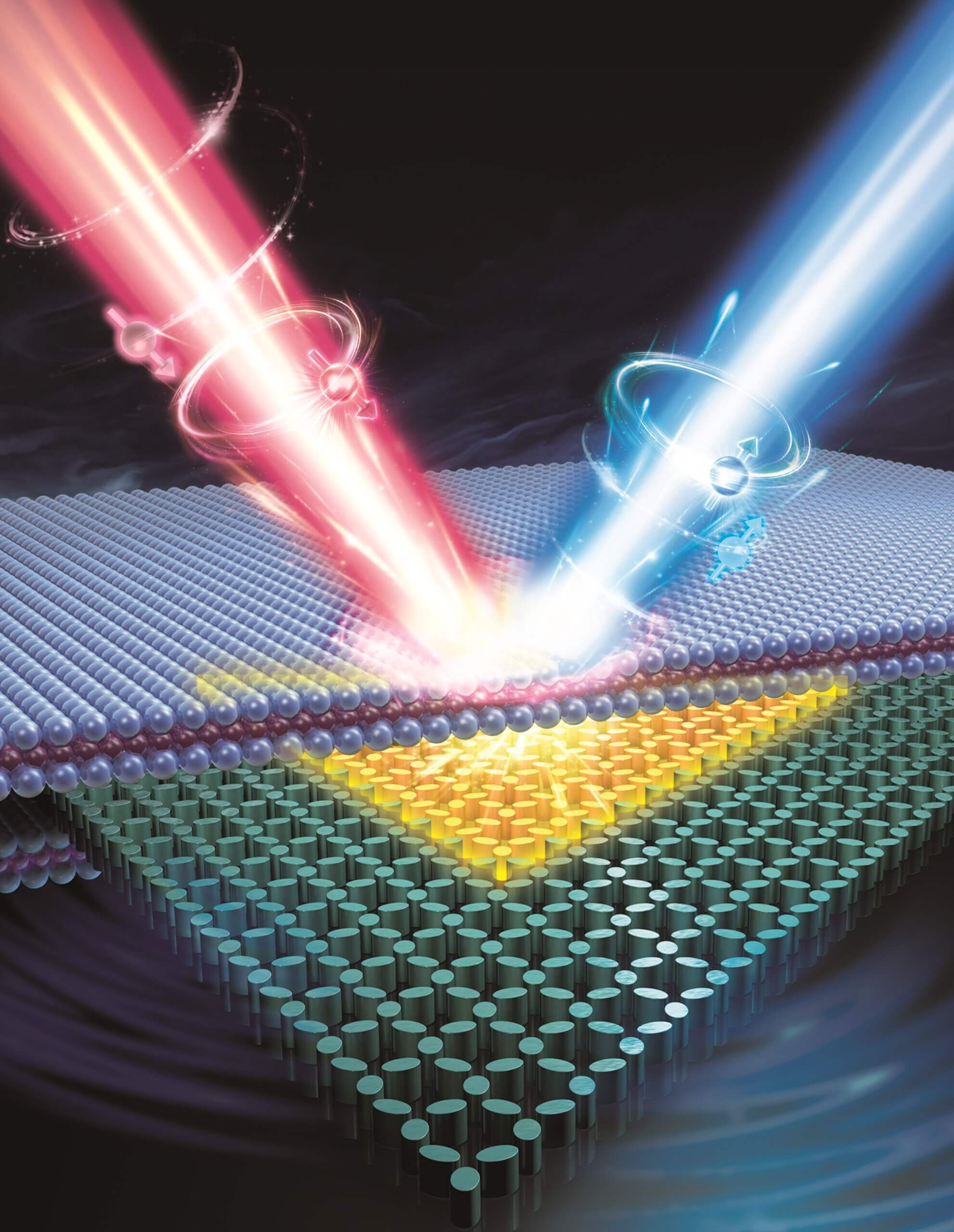
The discovery is based on the interaction of a single atomic layer with a two-dimensional resonator realized with the help of advanced nanotechnology. Electromagnetic waves (light), which also behave as massless particles called photons, have an internal property - "spin" of the photons. The spin, which is the internal angular momentum of the photons, depends on the direction of the circular polarization of the light. The research takes advantage of this feature of photons, paves the way for the study of spin-dependent coherent phenomena in both a classical and quantum context and opens new horizons for basic research and optoelectronic devices based on the spins of both electrons and photons.
The research was conducted in the research group of Prof. Erez Hasman, head of the Laboratory for Atomic Scale Photonics at the Technion, in collaboration with Prof. Elad Koren, head of the Laboratory for Electronic Nanomaterials and Nanocomponents at the Faculty of Materials Science and Engineering at the Technion, and Prof. Ariel Yashma from Tel Aviv University. The two research groups from the Technion maintain cooperation through the Russell Berry Institute for Nanotechnology at the Technion (RBNI) and the Helen Diller Quantum Center at the Technion. The research was carried out and led by Dr. Kexiu Rong, a post-doctoral student from Prof. Hasman's group, in collaboration with the following researchers:
Dr. Xiaoyang Duan, Dr. Bo Wang, Dr. Vladimir Kleiner, Dr. Assael Cohen, Dr. Pranab K. Mohapatra, Dr. Avinash Patsha, Dr. Subhrajit Mukherjee, Dror Reichenberg, Chieh-li Liu, and Vladi Gorovoy.
What are two-dimensional materials? According to Prof. Korn, "In 2004, the possibility of creating a single atomic layer was first examined when the physicists Andre Geim and Konstantin Novoslov, later winners of the Nobel Prize in Physics (2010), developed a simple method for creating single layers of carbon atoms. The two attached adhesive paper to a piece of graphite and peeled off the material layer by layer until obtaining a single layer of atoms known as graphene. They showed that the atomic layer of matter is very different in its properties from the properties of matter in its three-dimensional form. It is a material a hundred times stronger than steel and with extraordinary electrical properties, and according to estimates it is expected to revolutionize conductors and semiconductors, displays and screens, solar cells and more. Following this discovery, atomic layers were developed from other materials, and they also exhibited surprising and unique properties."
Prof. Hasman continues and explains: "Following the discovery of graphene, many two-dimensional materials were discovered and studied, such as various semiconductors, which also make it possible to obtain interesting optical properties. Standard electronic chips are based on silicon, which greatly limits the development of the next generation of computers that requires a combination of electronics and photonics, partly due to the lack of an essential condition called 'direct energy gap' in silicon. To our surprise, the same direct energy gap was discovered in two-dimensional semiconductors, which makes it possible to combine photonics and electronics on the nanometer scale, to produce light sources and active photonic devices with them, and to pave the way for future generations of chips."
To minimize the electronic chip and significantly increase the speed of processing and the rate of information transmission, the accepted approach today is spintronics - performing operations on the spin, one of the important properties of the electron, and not on the electron flow. A few years ago Prof. Erez Hasman founded a new field called spin-optics, which makes it possible to utilize the spin of the photons through metasurfaces for the benefit of transferring and processing information in photonic chips. The transfer of information is based on controlling the photonic spin with the help of nanophotonics - optics on the nanometer scale.
Dr. Qishu Rong explains, "Two-dimensional semiconductor materials are characterized by energy levels whose emission depends on spin, this is due to the breaking of the mirror symmetry. The researchers at the Technion decided to take advantage of this feature and attach a single atomic layer (WS2 For a two-dimensional (meta-surface) resonator based on nano-antennas that enable symmetry breaking in the photonic spin and receiving a laser from a chip on an atomic scale that enables a coherent and monochromatic light source while controlling and processing information in the photonic spin."
In 2020, the researchers from the Technion published in the journal Nature Nanotechnology ability to receive a light source"Regular" with spin properties from a two-dimensional material and an optical metasurface, when the photons were uncorrelated in incidence, wavelength and direction ("Like a flashlight with diffused light"), but the challenge that still remained was coordinating the photons and creating a spin laser that emits directed light, while using the two-dimensional material as a source of amplification by forced emission. Prof. Hasman points out that "we achieved this goal by creating an effective magnetic field that separates and controls the spin states of the laser in these dimensions, which does not require an additional system - a strong magnetic field to generate it (like the Zeeman or Faraday effect) and a temperature close to absolute zero, and the creation of a resonator which enables the existence of bikes with spin and minimal lost properties." As mentioned, their success paves the way for new ways to create tiny laser devices that may assist in the development of various and varied important applications.
Prof. Hasman proudly notes that "the current prestigious publication shows the importance of multidisciplinary research that combines physics, chemistry, materials science and engineering and the integration of international postdoctoral students in the research groups."
The research was supported by the National Science Foundation (ISF), and RBNI's Germ plan (research collaboration between the groups at the Technion). The components were realized at the Sara and Moshe Zisafel Center for Nanoelectronics (MNFU) at the Technion.
for the article in Nature Materials
More of the topic in Hayadan:
