Researchers at the Technion have engineered a material that may replace silicon in the world of electronics in the future; Through the stretching of the material at the atomic level, they gain control over the material's conduction and insulation properties, thus progressing towards turning it into a fast and efficient switch
Researchers at Viterbi's Faculty of Electrical and Computer Engineering have gained control of an innovative material that may replace silicon in the world of electronics in the future. This development is considered essential given the curbing of the miniaturization trend in the worlds of transistors and chips. The research was recently published in the scientific magazine Advanced Functional Materials.
Chips drive the world we live in - they are responsible for processing, storing and transmitting huge amounts of information. From the development of new drugs and the design of spacecraft engines to the servers that power the Internet - everything is based on chips.
The constant improvement in the capabilities of those chips is based on the constant minimization of the basic calculation units - transistors. These are tiny switches that control the passage of electric current, similar to a faucet that controls the flow of water. Through these switches the processor is able to perform its tasks: processing, storage (memory) and transfer of information.
Already in the mid-60s, Gordon Moore, the founder of Intel, stated that the rate of miniaturization of transistors would lead to the number of transistors on each given unit of area doubling every year and a half or two years. This prediction, which was based on the past (the development of transistors until 1965), dictated the rate of miniaturization for decades, and today chips are produced with billions of transistors in each. In 2007, Moore surprised himself when he said that there will never be resilience and that "Moore's Law" will come to an end in not many years. Moore himself passed away this year, when many in the technology world estimate that the law named after him is also nearing the end of its life.
Prof. Lior Kornblum, faculty member at the Viterbi Faculty of Electrical and Computer Engineering, explains that "as a result of constant miniaturization, transistors are now produced the size of a few tens of atoms. In these dimensions it is more and more difficult to continue miniaturization without harming the performance of the transistors and the chips that contain them. In nanometric sizes, the transistors behave in new ways, different from their larger ancestors, thus impairing the proper operation of the processor."
One of the examples of such disruptions is a leakage of electric current when the transistor (switch) is supposed to be off. According to Prof. Kornblum, "You can liken it to a leaking faucet. Such leakage in the transistor not only impairs performance but also leads to wastage of electricity. If we take for example a modern phone that contains billions of transistors, these tiny leaks will add up to significant energy loss, resulting in wasted energy (rapid battery drain) and significant heating of the device. If we move to orders of magnitude of server farms, the implications are enormous energy consumption and the release of a lot of heat into the atmosphere."
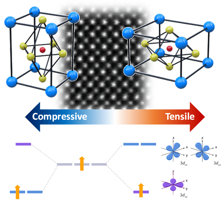
So how do you deal with the challenge? One of the promising directions is the search for alternative materials to silicon, the material from which transistors are made today. Prof. Kornblum's research group examines various oxides, one of which has a unique property - it can change its properties from an electrical conductor to an insulator and vice versa. The Technion researchers want to harness this feature in the future for the production of transistors that will close and open quickly.
How do you do it? Through precise control of the material and its atomic structure. The Technion researchers achieved control over the material's electrical properties through precise control of the distance between its atoms. The director of the laboratory Dr. Maria Baskin does this through a unique system for growing oxides; She "places" the atoms layer upon layer and thus grows the material in the laboratory. Thanks to the gentle and controlled growth process, it controls the distances between the atoms in a layer with a precision of a picometer, or a thousandth of a nanometer. For comparison, the distance between two atoms in silicon is about a quarter of a nanometer - 250 picometers. The unique growth system was established at the Technion with a large investment and will be used to develop the next generations of semiconductors, magnetic materials and materials for renewable energy such as advanced catalysts for energy conversion. "Every morning I come to the lab and start this system," says Dr. Baskin. "We can choose a variety of atom types and control their arrangement and the distances between them, thus creating materials that did not exist before, with a wide variety of properties as needed."
"The tools we developed for growing materials are unique on a global level," he says Prof. Lior Kornblom head Oxide Electronics Laboratory at the Sara and Moshe Zisafel Center for Nanoelectronics. "Growing the oxides is only the first step, and that's where the graduate students begin to carry out the research. Some focus on the physical properties of the materials to understand how they work and some harness these unique materials to make devices from them that will revolutionize microelectronics, renewable energy and more."
Doctoral student Lishi Shoma engages in her research in both fields together. She researches the properties of the material and produces a transistor from it to examine how it can be harnessed for the needs of microelectronics. In the current study, they led a team that included another 12 researchers from eight research institutions and companies located in Switzerland, Japan, France and the USA. The team led by her showed that by stretching the material at the atomic level it is possible to extend its chemical bonds; By stretching less than 2% in the length of the chemical bond, the researchers were able to "relax" the tendency of the electrons to jump from atom to atom. By these tiny changes, which occur in the range of a thousandth of a nanometer, the researchers are developing new ways to control the transition between the conducting and insulating states in this material. According to them, "It is amazing to see that such small changes in the atomic structure of the material have such a large effect on the properties of the material. We took this material to a particle accelerator in Switzerland and saw how these tiny changes affect the arrangement of the electrons in the material and the way they behave. These are exactly the tools we need to develop to create the transistors of the future. There are many challenges on the way there, and by controlling the arrangement of the electrons in the material we develop the abilities that will take us to the next level. Today I apply the research results to other similar materials, and from them I develop a new type of transistor."
According to Prof. Kornblum, "We have a great privilege to develop these abilities here in Israel, to work with brilliant students and to collaborate with leading scientists in the world who contributed to this research. We are reaping the fruits of the excellent scientific infrastructure that the Technion constantly develops and perfects, and of our excellent students."
The research was conducted at the Sarah and Moshe Zisafel Center for Nanoelectronics with funding from the National Science Foundation, and is supported by the Russell Berry Institute for Nanotechnology and the Nancy and Steven Grand Energy Program.
for the article in Advanced Functional Materials click here
More of the topic in Hayadan:

One response
Excellent and fascinating article.
Thank you.