Technion researchers answer this question and pave new paths for applications in communication, imaging and quantum computing
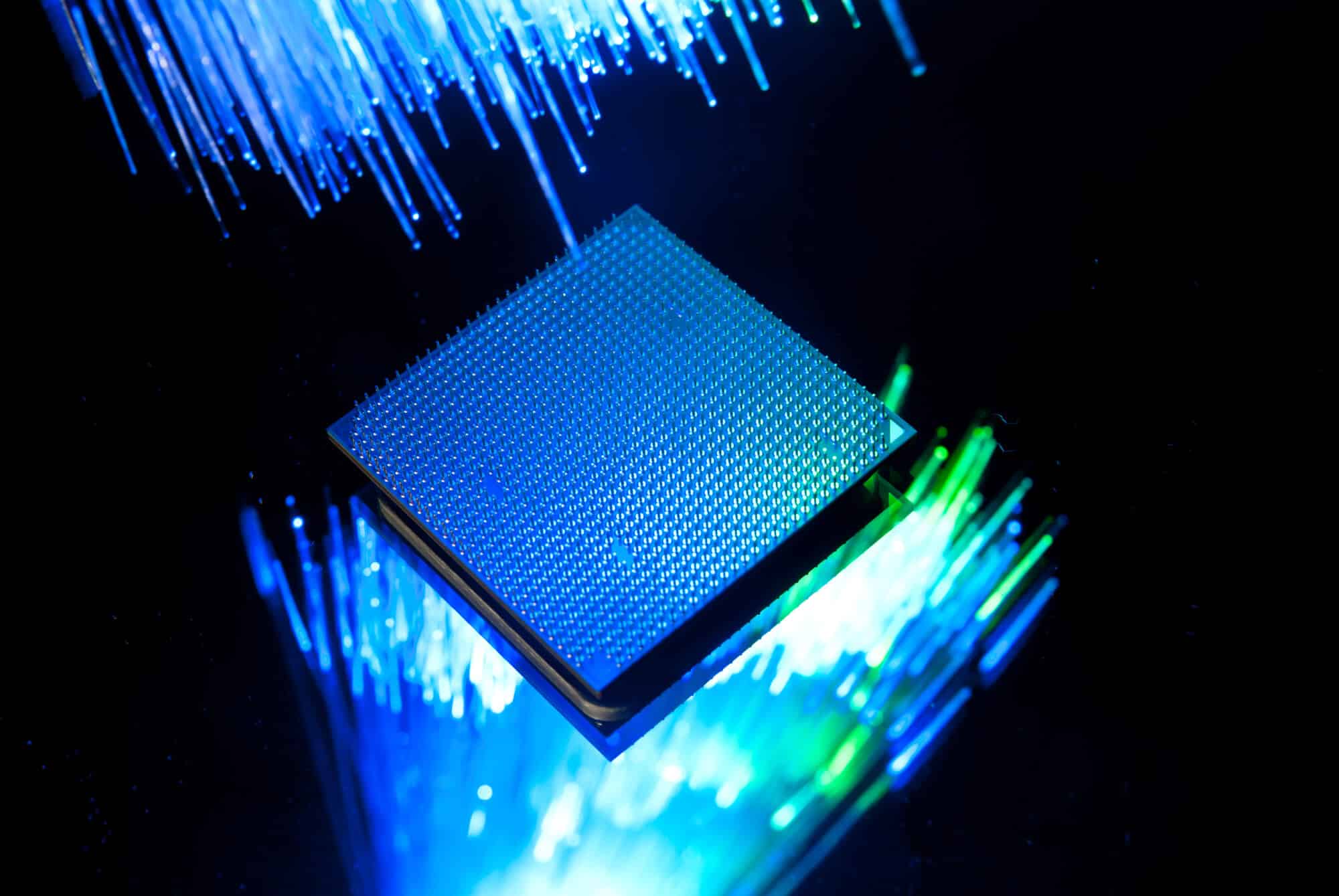
The field of photonic integrated circuits focuses on the miniaturization of photonic components and their implementation in photonic chips - circuits that perform a variety of computational operations in photons, and not in electrons as is the case in electronic circuits. Similar to chips in the world of electronics, also in photonic chips silicon is a very common raw material. Silicon-based photonics is an emerging field relevant to databases, artificial intelligence, quantum computing and more. It provides a leap forward in chip performance and cost-effectiveness. However, despite the high resolution of the manufacturing technologies (lithography), which allow for the precise production of the desired structures, the characterization tools still do not allow for accurate mapping of the optical properties of the chip, including the movement of light within it. The reason for this is the difficulty in modeling defects and inaccuracies in the material - a difficulty arising from the tiny dimensions of these standards.
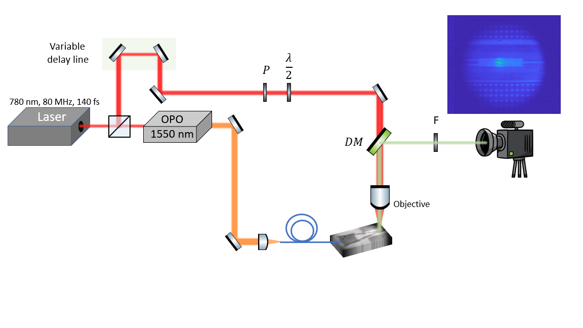
A new article by the researchers of the Viterbi Faculty of Electrical and Computer Engineering at the Technion deals with this challenge - the imaging of advanced light in photonic circuits on the chip. the research published in the journal OPTICAL It was led by the head of the Laboratory for Advanced Photonic Research Prof. Guy Bartel and the doctoral student Matan Iloz and the research group of Prof. Amir Rosenthal participated in it. The Technion researchers harnessed the optical properties of silicon to map the propagation of light within it, without the need for any invasive operation that changes the chip. This process includes mapping the electric field of the light waves and characterizing the elements that affect the movement of light - the waveguides and the beamsplitters.
The process developed by the Technion researchers provides imaging of the light inside the photonic chip in real time, without the need to damage the chip and without loss of data. This new process is expected to lead to the improvement of the design, production and optimization processes of photonic chips in a variety of fields including telecommunications, high performance computing, computational learning, measuring distances, medical imaging, sensing and quantum computing. Kobi Cohen, Yaakov Khair-Aldin, Yoav Hazan and Shay Tsass participated in the study.
The research was supported by the Helen Diller Center for Quantum Technologies at the Technion, the Center for Micro and Nano Electronics at the Technion and the Israel National Academy of Sciences.
More of the topic in Hayadan:
